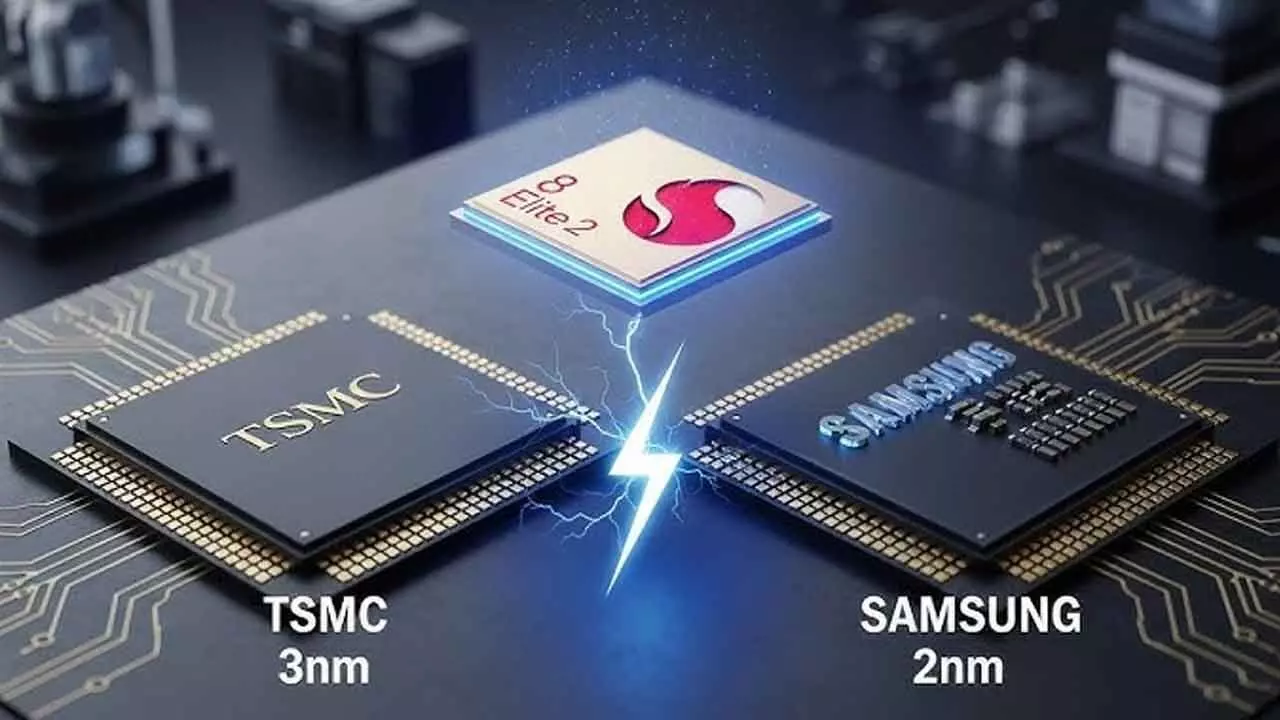
Qualcomm has announced the successful tape-out of its 2-nanometer semiconductor design, marking a major technological milestone for the company and underscoring India’s growing role in advanced chip development. The achievement was completed at Qualcomm’s Bengaluru design center, one of its largest engineering hubs outside the United States.
Tape-out represents the final stage of chip design before fabrication, signaling that the architecture is ready for manufacturing and large-scale testing.
Bengaluru’s Expanding Role in Global Chip Design
The announcement places Bengaluru firmly on the global semiconductor map, highlighting India’s evolution from a support base to a core innovation hub. Qualcomm’s engineers in the city played a central role in designing and validating the cutting-edge 2nm architecture, reflecting the depth of local expertise in advanced silicon engineering.
Industry observers note that this development aligns with India’s broader ambition to strengthen its semiconductor ecosystem through design, research, and manufacturing partnerships.
Why 2nm Matters for the Industry
The shift to 2nm technology is expected to deliver significant gains in performance, power efficiency, and transistor density compared to current 3nm and 4nm nodes. Chips built on this process can enable faster AI workloads, longer battery life in mobile devices, and improved efficiency in data centers and connected systems.
For Qualcomm, the milestone reinforces its competitive position in markets ranging from smartphones and PCs to automotive platforms and AI-driven edge computing.
Strategic Boost for India’s Semiconductor Ambitions
Qualcomm’s progress comes at a time when India is actively courting global chipmakers to expand local capabilities. The successful tape-out strengthens confidence in India’s ability to contribute meaningfully to next-generation semiconductor design, even as fabrication remains largely overseas.
Experts believe such milestones could accelerate further investments in advanced R&D centers and talent development across the country.
What Comes Next
Following tape-out, the 2nm design will move into fabrication and validation phases, where performance, yields, and power characteristics are closely evaluated. While Qualcomm has not disclosed a commercial launch timeline, the milestone suggests that next-generation products powered by 2nm technology are moving closer to reality.
 TECH TIMES NEWS