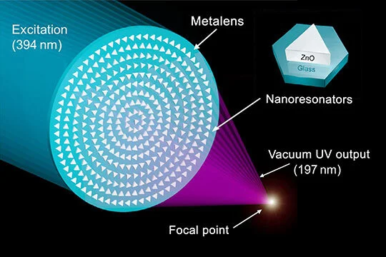
A team of researchers has developed a new class of ultra-compact, multi-layer lenses that could dramatically enhance the performance of portable optical devices. The innovation paves the way for sharper, lighter, and more efficient lenses in smartphones, drones, medical imaging tools, and compact cameras.
How the New Lens Works
The breakthrough centers on a stack of nanometer-thin optical layers that precisely control light at multiple wavelengths. Each layer acts as a microscopic filter, bending and focusing light with unprecedented accuracy. This allows the lens to overcome limitations of conventional single-layer metasurfaces, which often struggle with chromatic aberrations and limited focusing range.
Engineered with Advanced Nanofabrication Techniques
Using state-of-the-art nanofabrication, scientists layered different materials—such as silicon nitride and titanium dioxide—into intricate patterns measured in billionths of a meter. These multi-layer metasurfaces achieve remarkable optical control while remaining just a fraction of a millimeter thick, making them ideal for next-generation portable electronics.
Applications Across Multiple Fields
The new technology could revolutionize various sectors, including consumer electronics, biomedicine, and defense. Ultra-thin lenses could lead to flatter smartphone cameras, enhanced AR/VR headsets, and miniaturized endoscopic tools for non-invasive diagnostics. Moreover, the lenses’ precision and versatility make them suitable for satellite imaging and optical communication systems.
A Step Toward All-in-One Optical Chips
Researchers envision integrating these lenses into fully compact optical chips—combining imaging, sensing, and processing within a single platform. Such advancements could redefine the future of computational imaging and miniaturized optical instruments.
Future Outlook
While the technology remains in the experimental stage, its scalability and compatibility with existing semiconductor manufacturing make it promising for commercial adoption. The team aims to refine the design for mass production and explore integration with AI-driven imaging systems.
 TECH TIMES NEWS